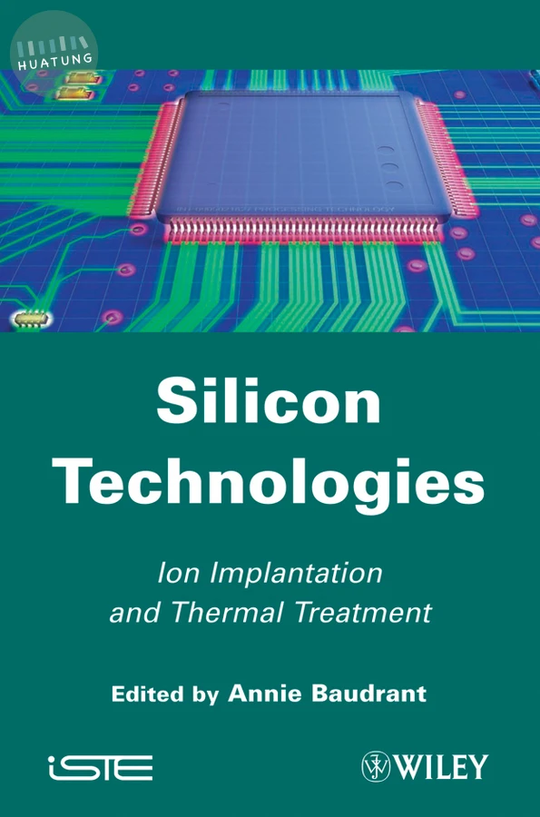
Silicon Technologies
$5387元 定價: $5985 9折 可訂購
簡介
This book has been written to provide newly arrived engineers in a silicon foundry environment with a comprehensive background in the fundamental physical and chemical basis for major front-end silicon treatments, such as oxidation, epitaxy, ion implantation and impurities diffusion, as well as giving a survey of the major types of equipment used in integrated circuit (IC) chip foundries.
Techniques include various forms of chemical vapor deposition (CVD), epitaxy, thin film technologies, lithography, masking, and other nanotechnologies.
As well as the target audience, the book will also be of great interest to engineers and advanced students in all these and related fields of electrical engineering, materials science, and manufacturing.
目錄
Preface xi
Annie BAUDRANT
Chapter 1. Silicon and Silicon Carbide Oxidation 1
Jean-Jacques GANEM and Isabelle TRIMAILLE
1.1. Introduction 1
1.2. Overview of the various oxidation techniques 3
1.3. Some physical properties of silica 17
1.4. Equations of atomic transport during oxidation 28
1.5. Is it possible to identify the transport mechanisms taking place during oxidation? 35
1.6. Transport equations in the case of thermal oxidation 48
1.7. Deal and Grove theory of thermal oxidation 53
1.8. Theory of thermal oxidation under water vapor of silicon 67
1.9. Kinetics of growth in O2 for oxide films < 30 nm 72
1.10. Fluctuations of the oxidation constants under experimental conditions 84
1.11. Conclusion 92
1.12. Bibliography 92
Chapter 2. Ion Implantation 103
Jean-Jacques GROB
2.1. Introduction 103
2.2. Ion implanters 105
2.3. Ion range 111
2.4. Creation and healing of the defects 124
2.5. Applications in traditional technologies and new tendencies 136
2.6. Conclusion 147
2.7. Bibliography 147
Chapter 3. Dopant Diffusion: Modeling and Technological Challenges 155
Daniel MATHIOT
3.1. Introduction 155
3.2. Diffusion in solids 157
3.3. Dopant diffusion in single-crystal silicon 176
3.4. Examples of associated engineering problems 191
3.5. Dopant diffusion in germanium 196
3.6. Conclusion 201
3.7. Bibliography 201
Chapter 4. Epitaxy of Strained Si/Si1-x Gex Heterostructures 209
Jean-Michel HARTMANN
4.1. Introduction 209
4.2. Engineering of the pMOSFET transistor channel using pseudomorphic SiGe layers 222
4.3. Engineering of the nMOSFET transistor channel using pseudomorphic Si1-yCy layers; SiGeC diffusion barriers
233
4.4. Epitaxy of Si raised sources and drains on ultra-thin SOI substrates 243
4.5. Epitaxy of recessed and raised SiGe:B sources and drains on ultra-thin SOI and SON substrates 248
4.6. Virtual SiGe substrates: fabrication of sSOI substrates and of dual c-Ge / t-Si channels 253
4.7. Thin or thick layers of pure Ge on Si for nano and opto-electronics 275
4.8. Devices based on sacrificial layers of SiGe 292
4.9. Conclusions and prospects 311
4.10. Bibliography 317
List of Authors 333
Index 335