搜尋建議
書名: Understanding Delta-Sigma Data Converters (2版)
作者: S.PAVAN R.SCHREIER
版次: 2
ISBN: 9781119258278
出版社: John Wiley
出版日期: 2017/01
書籍開數、尺寸: 24.5*16.7
重量: 0.92 Kg
頁數: 584
定價: 2080 元
售價: 2080
庫存: 現貨: >=5
查看店內位置
LINE US! 詢問這本書 團購優惠、書籍資訊 等

付款方式: 超商取貨付款 line pay
信用卡 全支付
線上轉帳 Apple pay
物流方式: 超商取貨
宅配
門市自取

【原文書】 書名:Understanding Delta-Sigma Data Converters 2/e 作者:S.PAVAN R.SCHREIER 出版社:JOHN WILEY 出版日期:2017/01/24 ISBN:9781119258278

大家的想法

還沒有人留下心得,快來搶頭香!

撰寫您的閱讀心得

為您推薦

Sigma-Delta Converters: Practical Design Guide (2版)

Sigma-Delta Converters: Practical Design Guide (2版)

其他會員也一起購買

【簡介】 Thoroughly revised and expanded to help readers systematically increase their knowledge and insight about Sigma-Delta Modulators Sigma-Delta Modulators (SDMs) have become one of the best choices for the implementation of analog/digital interfaces of electronic systems integrated in CMOS technologies. Compared to other kinds of Analog-to-Digital Converters (ADCs), Σ∆Ms cover one of the widest conversion regions of the resolution-versus-bandwidth plane, being the most efficient solution to digitize signals in an increasingly number of applications, which span from high-resolution low-bandwidth digital audio, sensor interfaces, and instrumentation, to ultra-low power biomedical systems and medium-resolution broadband wireless communications. Following the spirit of its first edition, Sigma-Delta Converters: Practical Design Guide, 2nd Edition takes a comprehensive look at SDMs, their diverse types of architectures, circuit techniques, analysis synthesis methods, and CAD tools, as well as their practical design considerations. It compiles and updates the current research reported on the topic, and explains the multiple trade-offs involved in the whole design flow of Sigma-Delta Modulators—from specifications to chip implementation and characterization. The book follows a top-down approach in order to provide readers with the necessary understanding about recent advances, trends, and challenges in state-of-the-art Σ∆Ms. It makes more emphasis on two key points, which were not treated so deeply in the first edition: It includes a more detailed explanation of Σ∆Ms implemented using Continuous-Time (CT) circuits, going from system-level synthesis to practical circuit limitations. It provides more practical case studies and applications, as well as a deeper description of the synthesis methodologies and CAD tools employed in the design of Σ∆ converters. Sigma-Delta Converters: Practical Design Guide, 2nd Edition serves as an excellent textbook for undergraduate and graduate students in electrical engineering as well as design engineers working on SD data-converters, who are looking for a uniform and self-contained reference in this hot topic. With this goal in mind, and based on the feedback received from readers, the contents have been revised and structured to make this new edition a unique monograph written in a didactical, pedagogical, and intuitive style. 【目錄】 Preface xix Acknowledgements xxv List of Abbreviations xxvii 1 Introduction to 𝚺𝚫 Modulators: Fundamentals, Basic Architecture and Performance Metrics 1 1.1 Basics of Analog-to-Digital Conversion 2 1.1.1 Sampling 3 1.1.2 Quantization 4 1.1.3 Quantization White Noise Model 5 1.1.4 Noise Shaping 8 1.2 Sigma-Delta Modulation 9 1.2.1 From Noise-shaped Systems to ΣΔ Modulators 10 1.2.2 Performance Metrics of ΣΔMs 11 1.3 The First-order ΣΔ Modulator 13 1.4 Performance Enhancement and Taxonomy of ΣΔMs 16 1.4.1 ΣΔM System-level Design Parameters and Strategies 17 1.4.2 Classification of ΣΔMs 18 1.5 Putting All The Pieces Together: From ΣΔMs to ΣΔ ADCs 19 1.5.1 Some Words about ΣΔ Decimators 20 1.6 ΣΔ DACs 22 1.6.1 System Design Trade-offs and Signal Processing in ΣΔ DACs 22 1.6.2 Implementation of Digital ΣΔMs used in DACs 24 1.7 Summary 25 References 26 2 Taxonomy of 𝚺𝚫 Architectures 29 2.1 Second-order ΣΔ Modulators 30 2.1.1 Alternative Representations of Second-order ΣΔMs 31 2.1.2 Second-Order ΣΔM with Unity STF 34 2.2 High-order Single-loop ΣΔMs 35 2.3 Cascade ΣΔ Modulators 39 2.3.1 SMASH ΣΔM Architectures 46 2.4 Multi-bit ΣΔ Modulators 49 2.4.1 Influence of Multi-bit DAC Errors 49 2.4.2 Dynamic Element Matching Techniques 50 2.4.3 Dual Quantization 53 2.4.3.1 Dual-quantization Single-loop ΣΔMs 53 2.4.3.2 Dual-quantization Cascade ΣΔMs 54 2.5 Band-pass ΣΔ Modulators 55 2.5.1 Quadrature BP-ΣΔMs 56 2.5.2 The z → −z2 LP–BP Transformation 58 2.5.3 BP-ΣΔMs with Optimized NTF 58 2.5.4 Time-interleaved and Polyphase BP-ΣΔMs 61 2.6 Continuous-time ΣΔ Modulators: Architecture and Basic Concepts 64 2.6.1 An Intuitive Analysis of CT-ΣΔMs 66 2.6.2 Some Words about Alias Rejection in CT-ΣΔMs 69 2.7 DT–CT Transformation of ΣΔMs 70 2.7.1 The Impulse-invariant Transformation 70 2.7.2 DT–CT Transformation of a Second-order ΣΔM 72 2.8 Direct Synthesis of CT-ΣΔMs 74 2.9 Summary 76 References 76 3 Circuit Errors in Switched-capacitor 𝚺𝚫 Modulators 83 3.1 Overview of Nonidealities in Switched-capacitor ΣΔ Modulators 84 3.2 Finite Amplifier Gain in SC-ΣΔMs 86 3.3 Capacitor Mismatch in SC-ΣΔMs 90 3.4 Integrator Settling Error in SC-ΣΔMs 91 3.4.1 Behavioral Model for the Integrator Settling 91 3.4.2 Linear Effect of Finite Amplifier Gain–Bandwidth Product 95 3.4.3 Nonlinear Effect of Finite Amplifier Slew Rate 98 3.4.4 Effect of Finite Switch On-resistance 100 3.5 Circuit Noise in SC-ΣΔMs 101 3.6 Clock Jitter in SC-ΣΔMs 105 3.7 Sources of Distortion in SC-ΣΔMs 107 3.7.1 Nonlinear Amplifier Gain 107 3.7.2 Nonlinear Switch On-Resistance 109 3.8 Case Study: High-level Sizing of a ΣΔM 111 3.8.1 Ideal Modulator Performance 111 3.8.2 Noise Leakages 112 3.8.3 Circuit Noise 115 3.8.4 Settling Error 116 3.8.5 Overall High-Level Sizing and Noise Budget 117 3.9 Summary 119 References 119 4 Circuit Errors and Compensation Techniques in Continuous-time 𝚺𝚫 Modulators 123 4.1 Overview of Nonidealities in Continuous-time ΣΔ Modulators 123 4.2 CT Integrators and Resonators 124 4.3 Finite Amplifier Gain in CT-ΣΔMs 126 4.4 Time-constant Error in CT-ΣΔMs 128 4.5 Finite Integrator Dynamics in CT-ΣΔMs 130 4.5.1 Effect of Finite Gain–Bandwidth Product on CT-ΣΔMs 131 4.5.2 Effect of Finite Slew Rate on CT-ΣΔMs 133 4.6 Sources of Distortion in CT-ΣΔMs 134 4.6.1 Nonlinearities in the Front-end Integrator 134 4.6.2 Intersymbol Interference in the Feedback DAC 136 4.7 Circuit Noise in CT-ΣΔMs 137 4.7.1 Noise Analysis Considering NRZ Feedback DACs 137 4.7.2 Noise Analysis Considering SC Feedback DACs 139 4.8 Clock Jitter in CT-ΣΔMs 140 4.8.1 Jitter in Return-to-zero DACs 141 4.8.2 Jitter in Non-return-to-zero DACs 142 4.8.3 Jitter in Switched-capacitor DACs 144 4.8.4 Lingering Effect of Clock Jitter Error 145 4.8.5 Reducing the Effect of Clock Jitter with FIR and Sine-shaped DACs 147 4.9 Excess Loop Delay in CT-ΣΔMs 149 4.9.1 Intuitive Analysis of ELD 149 4.9.2 Analysis of ELD based on Impulse-invariant DT-CT Transformation 151 4.9.3 Alternative ELD Compensation Techniques 154 4.10 Quantizer Metastability in CT-ΣΔMs 155 4.11 Summary 159 References 160 5 Behavioral Modeling and High-level Simulation 165 5.1 Systematic Design Methodology of ΣΔ Modulators 165 5.1.1 System Partitioning and Abstraction Levels 167 5.1.2 Sizing Process 167 5.2 Simulation Approaches for the High-level Evaluation of ΣΔMs 169 5.2.1 Alternatives to Transistor-level Simulation 169 5.2.2 Event-driven Behavioral Simulation Technique 171 5.2.3 Programming Languages and Behavioral Modeling Platforms 172 5.3 Implementing ΣΔM Behavioral Models 173 5.3.1 From Circuit Analysis to Computational Algorithms 173 5.3.2 Time-domain versus Frequency-domain Behavioral Models 175 5.3.3 Implementing Time-domain Behavioral Models in MATLAB 178 5.3.4 Building Time-domain Behavioral Models as SIMULINK C-MEX S-functions 182 5.4 Efficient Behavioral Modeling of ΣΔM Building Blocks using C-MEX S-functions 188 5.4.1 Modeling of SC Integrators using S-functions 188 5.4.1.1 Capacitor Mismatch and Nonlinearity 190 5.4.1.2 Input-referred Thermal Noise 191 5.4.1.3 Switch On-resistance Dynamics 194 5.4.1.4 Incomplete Settling Error 197 5.4.2 Modeling of CT Integrators using S-functions 200 5.4.2.1 Single-pole Gm-C Model 200 5.4.2.2 Two-pole Dynamics Model 201 5.4.2.3 Modeling Transconductors as S-functions 203 5.4.3 Behavioral Modeling of Quantizers using S-functions 205 5.4.3.1 Modeling Multi-level ADCs as S-functions 205 5.4.3.2 Modeling Multi-level DACs as S-functions 207 5.5 SIMSIDES: A SIMULINK-based Behavioral Simulator for ΣΔMs 209 5.5.1 Model Libraries Included in SIMSIDES 210 5.5.2 Structure of SIMSIDES and its User Interface 211 5.5.2.1 Creating a New ΣΔM Block Diagram 212 5.5.2.2 Setting Model Parameters 215 5.5.2.3 Simulation Analyses 215 5.6 Using SIMSIDES for High-level Sizing and Verification of ΣΔMs 216 5.6.1 SC Second-order Single-Bit ΣΔM 216 5.6.1.1 Effect of Amplifier Finite DC Gain 218 5.6.1.2 Effect of Thermal Noise 218 5.6.1.3 Effect of the Incomplete Settling Error 220 5.6.1.4 Cumulative Effect of All Errors 221 5.6.2 CT Fifth-order Cascade 3-2 Multi-bit ΣΔM 224 5.6.2.1 Effect of Nonideal Effects 227 5.6.2.2 High-level Synthesis and Verification 229 5.7 Summary 231 References 231 6 Automated Design and Optimization of 𝚺𝚫Ms 235 6.1 Architecture Exploration and Selection: Schreier’s Toolbox 236 6.1.1 Basic Functions of Schreier’s Delta-Sigma Toolbox 236 6.1.2 Synthesis of a Fourth-order CRFF LP/BP SC-ΣΔM with Tunable Notch 238 6.1.3 Synthesis of a Fourth-order BP CT-ΣΔM with Tunable Notch 240 6.2 Optimization-based High-level Synthesis of ΣΔ Modulators 245 6.2.1 Combining Behavioral Simulation and Optimization 246 6.2.2 Using Simulated Annealing as Optimization Engine 247 6.2.3 Combining SIMSIDES with MATLAB Optimizers 253 6.3 Lifting Method and Hardware Acceleration to Optimize CT-ΣΔMs 255 6.3.1 Hardware Emulation of CT-ΣΔMs on an FPGA 257 6.3.2 GPU-accelerated Computing of CT-ΣΔMs 258 6.4 Using Multi-objective Evolutionary Algorithms to Optimize ΣΔMs 259 6.4.1 Combining MOEA with SIMSIDES 261 6.4.2 Applying MOEA and SIMSIDES to the Synthesis of CT-ΣΔMs 262 6.5 Summary 269 References 269 7 Electrical Design of 𝚺𝚫Ms: From Systems to Circuits 271 7.1 Macromodeling ΣΔMs 272 7.1.1 SC Integrator Macromodel 272 7.1.1.1 Switch Macromodel 272 7.1.1.2 OTA Macromodel 274 7.1.2 CT Integrator Macromodel 274 7.1.2.1 Active-RC Integrators 274 7.1.2.2 Gm-C Integrators 274 7.1.3 Nonlinear OTA Transconductor 275 7.1.4 Embedded Flash ADC Macromodel 276 7.1.5 Feedback DAC Macromodel 277 7.2 Examples of ΣΔM Macromodels 279 7.2.1 SC Second-order Example 279 7.2.2 Second-order Active-RC ΣΔM 283 7.3 Including Noise in Transient Electrical Simulations of ΣΔMs 286 7.3.1 Generating and Injecting Noise Data Sequences in HSPICE 287 7.3.2 Analyzing the Impact of the Main Noise Sources in SC Integrators 289 7.3.3 Generating and Injecting Flicker Noise Sources in Electrical Simulations 289 7.3.4 Test Bench to Include Noise in the Simulation of ΣΔMs 293 7.4 Processing ΣΔM Output Results of Electrical Simulations 294 7.5 Summary 298 References 298 8 Design Considerations of 𝚺𝚫M Subcircuits 301 8.1 Design Considerations of CMOS Switches 302 8.1.1 Trade-Off Between Ron and the CMOS Switch Drain/Source Parasitic Capacitances 302 8.1.2 Characterizing the Nonlinear Behavior of Ron 302 8.1.3 Influence of Technology Downscaling on the Design of Switches 304 8.1.4 Evaluating Harmonic Distortion due to CMOS Switches 305 8.2 Design Considerations of Operational Amplifiers 308 8.2.1 Typical Amplifier Topologies 309 8.2.2 Common-mode Feedback Networks 311 8.2.3 Characterization of the Amplifier in AC 313 8.2.4 Characterization of the Amplifier in DC 313 8.2.5 Characterization of the Amplifier Gain Nonlinearity 316 8.3 Design Considerations of Transconductors 317 8.3.1 Highly Linear Front-end Transconductor 318 8.3.2 Loop-filter Transconductors 320 8.3.3 Widely Programmable Transconductors 323 8.4 Design Considerations of Comparators 324 8.4.1 Regenerative Latch-based Comparators 325 8.4.2 Design Guidelines of Comparators 327 8.4.3 Characterization of Offset and Hysteresis Based on the Input-ramp Method 328 8.4.4 Characterization of Offset and Hysteresis Based on the Bisectional Method 328 8.4.5 Characterizing the Comparison Time 330 8.5 Design Considerations of Current-Steering DACs 332 8.5.1 Fundamentals and Basic Concepts of CS DACs 333 8.5.2 Practical Realization of CS DACs 333 8.5.3 Current Cell Circuits, Error Limitations, and Design Criteria 336 8.5.4 CS 4-bit DAC Example 336 8.6 Summary 338 References 338 9 Practical Realization of 𝚺𝚫Ms: From Circuits to Chips 341 9.1 Auxiliary ΣΔM Building Blocks 341 9.1.1 Clock-phase Generators 342 9.1.1.1 Phase Generation 342 9.1.1.2 Phase Buffering 342 9.1.1.3 Phase Distribution 344 9.1.2 Generation of Common-mode Voltage, Reference Voltage, and Bias Currents 345 9.1.2.1 Bandgap Circuit 345 9.1.2.2 Reference Voltage Generator 345 9.1.2.3 Master Bias Current Generator 346 9.1.2.4 Common-mode Voltage Generator 346 9.1.3 Additional Digital Logic 347 9.2 Layout Design, Floorplanning, and Practical Issues 348 9.2.1 Layout Floorplanning 348 9.2.1.1 Divide Layout into Different Parts or Regions 348 9.2.1.2 Shield Sensitive ΣΔM Analog Subcircuits from Switching Noise 349 9.2.1.3 Buses to Distribute Signals Shared by Different ΣΔM Parts 349 9.2.1.4 Be Obsessive about Layout Symmetry and Details of Analog Parts 349 9.2.2 I/O Pad Ring 350 9.2.3 Importance of Layout Verification and Catastrophic Failure 350 9.3 Chip Package, Test PCB, and Experimental Setup 354 9.3.1 Bonding Diagram and Package 354 9.3.2 Test PCB 355 9.4 Experimental Test Set-Up 355 9.4.1 Planning the Type and Number of Instruments Needed 357 9.4.2 Connecting Lab Instruments 357 9.4.3 Measurement Set-Up Example 358 9.5 ΣΔM Design Examples and Case Studies 359 9.5.1 Programmable-gain ΣΔMs for High Dynamic Range Sensor Interfaces 360 9.5.1.1 Main Design Criteria and Performance Limitations 361 9.5.1.2 SC Realization with Programmable Gain and Double Sampling 362 9.5.1.3 Influence of Chopper Frequency on Flicker Noise 362 9.5.2 Reconfigurable SC-ΣΔMs for Multi-standard Direct Conversion Receivers 364 9.5.2.1 Power-scaling Circuit Techniques 367 9.5.2.2 Experimental Results 368 9.5.3 Using Widely-programmable Gm-LC BP-ΣΔMs for RF Digitizers 368 9.5.3.1 Application Scenario 371 9.5.3.2 Gm-LC BP-ΣΔM High-level Sizing 371 9.5.3.3 BP CT-ΣΔM Loop-Filter Reconfiguration Techniques 375 9.5.3.4 Embedded 4-bit Quantizer with Calibration 378 9.5.3.5 Biasing, Digital Control Programmability and Testability 382 9.6 Summary 385 References 386 10 Frontiers, Trends and Challenges: Towards Next-generation 𝚺𝚫 Modulators 389 10.1 State-of-the-Art ADCs: Nyquist-rate versus ΣΔ Converters 390 10.1.1 Conversion Energy 391 10.1.2 Figures of Merit 392 10.2 Comparison of Different Categories of ΣΔ ADCs 393 10.2.1 Aperture Plot of ΣΔMs 406 10.2.2 Energy Plot of ΣΔMs 407 10.3 Empirical and Statistical Analysis of State-of-the-Art ΣΔMs 408 10.3.1 SC versus CT ΣΔMs 408 10.3.2 Technology used in State-of-the-Art ΣΔMs 410 10.3.3 Single-Loop versus Cascade ΣΔMs 410 10.3.4 Single-bit versus Multi-bit ΣΔMs 411 10.3.5 Low-pass versus Band-pass ΣΔMs 413 10.3.6 Emerging ΣΔM Techniques 415 10.4 Gigahertz-range ΣΔMs for RF-to-digital Conversion 415 10.5 Enhanced Cascade ΣΔMs 418 10.5.1 SMASH CT-ΣΔMs 418 10.5.2 Two-stage 0-L MASH 419 10.5.3 Stage-sharing Cascade ΣΔMs 420 10.5.4 Multi-rate and Hybrid CT/DT ΣΔMs 420 10.5.4.1 Upsampling Cascade MR-ΣΔMs 421 10.5.4.2 Downsampling Hybrid CT/DT Cascade MR-ΣΔMs 422 10.6 Power-efficient ΣΔM Loop-filter Techniques 423 10.6.1 Inverter-based ΣΔMs 423 10.6.2 Hybrid Active/Passive and Amplifier-less ΣΔMs 424 10.6.3 Power-efficient Amplifier Techniques 426 10.7 Hybrid ΣΔM/Nyquist-rate ADCs 428 10.7.1 Multi-bit ΣΔM Quantizers based on Nyquist-rate ADCs 428 10.7.2 Incremental ΣΔ ADCs 429 10.8 Time-based ΣΔ ADCs 431 10.8.1 ΣΔMs with VCO/PWM-based Quantization 432 10.8.2 Scaling-friendly Mostly-digital ΣΔMs 433 10.8.3 GRO-based ΣΔMs 434 10.9 DAC Techniques for High-performance CT-ΣΔMs 436 10.10 Classification of State-of-the-Art References 437 10.11 Summary and Conclusions 437 References 438 A State-space Analysis of Clock Jitter in CT-𝚺𝚫Ms 463 A.1 State-space Representation of NTF (z) 463 A.2 Expectation Value of (Δqn)2 465 A.3 In-band Noise Power due to Clock Jitter 466 References 467 B SIMSIDES User Guide 469 B.1 Getting Started: Installing and Running SIMSIDES 470 B.2 Building and Editing ΣΔM Architectures in SIMSIDES 470 B.3 Analyzing ΣΔMs in SIMSIDES 473 B.3.1 Node Spectrum Analysis 474 B.3.2 Integrated Power Noise 474 B.3.3 SNR/SNDR 475 B.3.4 Harmonic Distortion 475 B.3.5 Integral and Differential Non-Linearity 477 B.3.6 Multi-tone Power Ratio 477 B.3.7 Histogram 478 B.3.8 Parametric Analysis 478 B.3.9 Monte Carlo Analysis 479 B.4 Optimization Interface 480 B.5 Tutorial Example: Using SIMSIDES to Model and Analyze ΣΔMs 482 B.5.1 Creating the Cascade 2-1 ΣΔM Block Diagram in SIMSIDES 482 B.5.2 Setting Model Parameters 482 B.5.3 Computing the Output Spectrum 484 B.5.4 SNR versus Input Amplitude Level 486 B.5.5 Parametric Analysis Considering Only One Parameter 487 B.5.6 Parametric Analysis Considering Two Parameters 488 B.5.7 Computing Histograms 489 B.6 Getting Help 489 C SIMSIDES Block Libraries and Models 491 C.1 Overview of SIMSIDES Libraries 491 C.2 Ideal Libraries 492 C.2.1 Ideal Integrators 492 C.2.1.1 Building-block Model Purpose and Description 492 C.2.1.2 Model Parameters 493 C.2.2 Ideal Resonators 493 C.2.2.1 Ideal_LD_Resonator 493 C.2.2.2 Ideal_FE_Resonator 493 C.2.2.3 Ideal_CT_Resonator 493 C.2.3 Ideal Quantizers 494 C.2.3.1 Ideal_Comparator 494 C.2.3.2 Ideal_Comparator_for_SI 495 C.2.3.3 Ideal_Multibit_Quantizer 495 C.2.3.4 Ideal_Multibit_Quantizer_for_SI 496 C.2.3.5 Ideal_Multibit_Quantizer_levels 496 C.2.3.6 Ideal_Multibit_Quantizer_levels_SD2 496 C.2.3.7 Ideal_Sampler 496 C.2.4 Ideal D/A Converters 496 C.2.4.1 Ideal_DAC_for_SI 496 C.2.4.2 Ideal_DAC_dig_level_SD2 497 C.3 Real SC Building-Block Libraries 497 C.3.1 Real SC Integrators 497 C.3.2 Real SC Resonators 501 C.4 Real SI Building-Block Libraries 503 C.4.1 Real SI Integrators 503 C.4.2 Real SI Resonators 505 C.4.3 SI Errors and Model Parameters 506 C.4.3.1 Basic_SI_FE(LD)_Integrator and Basic_SI_FE(LD)_Resonator 506 C.4.3.2 SI_FE(LD)_Int_Finite_Conductance 507 C.4.3.3 SI_FE(LD)_Int_Finite_Conductance & Settling & ChargeInjection 508 C.5 Real CT Building-Block Libraries 508 C.5.1 Real CT Integrators 508 C.5.1.1 Model Parameters used in Transconductors and Gm-C Integrator Building Blocks 511 C.5.1.2 Gm-MC Integrators 511 C.5.1.3 Active-RC Integrators 512 C.5.1.4 MOSFET-C Integrators 513 C.5.2 Real CT Resonators 513 C.5.2.1 Gm-C Resonators 514 C.5.2.2 Gm-LC Resonators 517 C.6 Real Quantizers & Comparators 517 C.7 Real D/A Converters 518 C.8 Auxiliary Blocks 519 Index 523

原價: 1950 售價: 1950 現省: 0元
立即查看
ANALOG IC DESIGN WITH LOW-DROPOUT REGULATORS (2版)

ANALOG IC DESIGN WITH LOW-DROPOUT REGULATORS (2版)

其他會員也一起購買

<姆斯>ANALOG IC DESIGN WITH LOW-DROPOUT REGULATORS 2E 2014 (I.E.) <McGraw-Hill> 2/E RINCON-MORA 9789863411239

原價: 1080 售價: 1080 現省: 0元
立即查看
類比CMOS積分電路設計詳解 (1版)

類比CMOS積分電路設計詳解 (1版)

其他會員也一起購買

【書籍印製時偶有輕微墨點,不介意再下單】 類比CMOS積分電路設計習題詳解 ISBN13:9789571206523 出版社:曉園 作者:B. RAZAVI 裝訂:平裝 出版日:2007/06/01 中國圖書分類:電氣工程 內容簡介 研習理工的同學,都有一種認識,那就是,一本書的習題往往是該書的精華所在,藉著習題的印證,才能對書中的原理原則徹底的吸收與了解。 有鑒於此,曉園出版社特地請了許多在本科上具有相當研究與成就的人士,精心出版了一系列的題解叢書,為各該科目的研習,作一番介紹與鋪路的工作。 一個問題的解答方法,常因思惟的角度而異。曉園題解叢書,毫無疑問的都是經過一番精微的思考與分析而得。其目的在提供對各該科目研讀時的參考與比較;而對於一般的自修者,則有啟發與提示的作用。希望讀者能藉這一系列題解叢書的幫助,而在本身的學問進程上有更上層樓的成就。

原價: 280 售價: 280 現省: 0元
立即查看
新日檢完勝單語N3(附MP3+免費APP試題) (1版)

新日檢完勝單語N3(附MP3+免費APP試題) (1版)

其他會員也一起購買

3大理由,這本N3單字書非用不可! 理由一:專業製作搭檔! アークアカデミー東京校執筆+日本アスク集團出版+東京腔師資朗讀錄音 理由二:記單字有訣竅! 依「主題」串聯必考單字,「讀解」、「聽解」科目無形中一起進步! 理由三:免費APP模擬試題,自我測驗! 「字彙模擬試題」,打開APP就能做,挑戰實力不用多掏錢; 「單字、例句朗讀」,打開APP就能聽,躺著、坐著、站著都能輕鬆複習! 一定考上?絕對合格?完全攻略?第一次買日檢單字書的人看這裡! 好的語言教材,當然不是隨便一位母語者就能寫得出來。 本書由アークアカデミー東京校老師執筆、校長監修,日本專業語言教材出版社ASK(アスク)編輯出版,並在日本當地錄製標準東京腔。如果你對市面上一堆「一定考上」「絕對合格」「完全攻略」的書感到困惑、不知如何抉擇的話,本書以專業教學立場精挑必學單字,即使不為考試,也是生活必備單字。 想利用背單字,同時提升「聽解」、「讀解」能力嗎? 按照50音順序背單字,容易背過就忘?如果你不擅長硬背單字,那麼試試依照主題來記吧!アークアカデミー東京校團隊從教學經驗中發現,即使是檢定單字,經過主題、情境分類,記憶效果最好,尤其「聽解」、「讀解」兩科目試題通常也各有主題,如「天氣」「興趣」「家人」「數據表格」等,因此透過主題背過的單字,考生較能迅速回想,立即反應。 想爭取讀書時間、節省荷包嗎? 「眾文新日檢」免費APP,針對日檢「每個等級」(N1~N5)額外提供書裡沒有的「字彙模擬試題」,打造你的完勝進修計畫。模擬試題完全免費,APP中亦包含書中所有單字、例句朗讀音檔,學習不再受地點、工具限制,任何時候躺著、站著、等人、運動、通勤皆可複習!

原價: 350 售價: 298 現省: 52元
立即查看
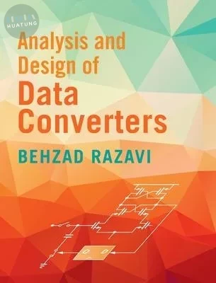
Analysis and Design of Data Converters (1版)

Analysis and Design of Data Converters (1版)

其他會員也一起購買

【簡介】 Master the art of data converter design with this definitive textbook, a detailed and accessible introduction ideal for students and practicing engineers. Razavi’s distinctive and intuitive pedagogical approach, building up from elementary components to complex systems. Step-by-step transistor-level designs and simulations offer a practical hands-on understanding of key design concepts. Comprehensive coverage of essential topics including sampling circuits, comparator design, digital-to-analog converters, flash topologies, SAR and pipelined architectures, time-interleaved converters, and oversampling systems. Over 250 examples pose thought-provoking questions, reinforcing core concepts and helping students develop confidence. Over 350 end-of-chapter homework problems to test student understanding, with solutions available for course instructors. Developed by leading author Behzad Razavi, and addressing all the principles and design concepts essential to today’s engineers, this is the ideal text for senior undergraduate and graduate-level students and professional engineers who aspire to excel in data converter analysis and design.

原價: 1980 售價: 1940 現省: 40元
立即查看
TRY!日本語N2達陣:從日檢文法展開 (1版)

TRY!日本語N2達陣:從日檢文法展開 (1版)

其他會員也一起購買

日檢TOP 1!百萬考生實證推薦的超效學習法 「日語課本」與「日檢備考」合而為一的全新教材! 將N2必備文法融入課文, 以日檢「文法」「聽解」「讀解」出題形式設計練習題, 在學習日語的過程中,同時準備日檢,成功達陣! 「TRY!日本語能力試験 文法から伸ばす日本語」系列為ABK(公益財団法人アジア学生文化協会)以其35年的日語教育經驗編纂而成。編寫期間,也同時作為旗下日本語學校的授課教材,因而經過實際教學的反覆驗證,是目前將日檢文法整理得最完備的實用教材,讓讀者在學習日語的過程中能同時熟悉日檢題型,事半功倍,深獲第一線教師們高度肯定! 本書完整規劃14章、139個 N2必學文法項目,每章分配4~8個項目,方便讀者自學或課堂教學安排進度。 特色1:實用文法,真正能運用在生活中 本書以日檢「Can-do」精神,將日檢文法融入各種生活情境中,如天氣預報、科普文章、美食新聞、商品開發、演講致詞等,實用生動的會話或文章,搭配可愛的插圖,文法不再枯燥,讓學習者能將課本所學實際運用在日常生活中。 特色2:重要觀念圖示化,化繁為簡,學習更有效 本書將重要觀念視覺圖示化,讀者一看就懂。如文法最重視的「接續」說明,以公式化呈現。每項文法的重要程度以星號★標示,星號越多表示越重要。此外,將句型的使用場合,用符號提示親疏遠近、正式∕非正式、口語∕書面語,幫助學習者了解日語的正確用法,才不致於發生看似語法正確、其實用法錯誤的日文。 特色3:延伸學習相似句型,點線面完全提升 當日文程度越好時,對於相似句型的文法細節往往更容易混淆。每個文法解說皆再提供數個相關例句輔助說明,學習者可更加熟悉文法內容。若例句延伸出其他文法觀念或易混淆句型,書裡也會標示相關參考的頁碼,讀者可立即查詢,相互參照,加深記憶。 號稱文法界祕笈的「相似句型一覽表」,除了把 N2級別以下相似的文法句型整理出來,還有級數、句型編號和對應的課本頁數!方便學習者查詢對照,融會貫通。 特色4:大量練習,日檢題型融入學習中 為求最佳的學習成果,書中設計大量練習題目,幫助學習者找出不足之處。每個章節「Check單元」,提供簡單的練習題目,務必釐清該章的文法觀念。在每章結束後還有綜合測驗(もとめの問題),特別的是,作者採用日檢三科的出題形式,學習者在複習時,「文法」、「聽解」、「讀解」的作答能力也可同步提升。 免費超值下載 ■ MP3音檔:內含課文朗讀音檔、聽力試題音檔。 ■ 課文單字表:將書中N2必學單字製作成表,讀者可自行下載,重點單字總整理,加速記憶,搭配課本使用效果最好。

原價: 380 售價: 323 現省: 57元
立即查看
Linear Algebra: A Modern Introduction (5版)

Linear Algebra: A Modern Introduction (5版)

其他會員也一起購買

【簡介】 ●A CLEAR WRITING STYLE that is simple, direct and conversational, while maintaining rigorous proof coverage, is present. ●AVAILABLE WITH WEBASSIGN, the text will help your students build problem-solving skills and develop conceptual understanding. ●EXPLORATONS AND WRITING PROJECTS designed for individual or group work provide hands-on learning opportunities. Explorations are available to assign within WebAssign. ●A VARIETY OF NUMERICAL LINEAR ALGEBRA TECHNIQUES are included such as pivoting strategies and iterative methods for solving linear systems. 【目錄】 Chapter 1: Vectors Chapter 2: Systems of Linear Equations Chapter 3: Matrices Chapter 4: Eigenvalues and Eigenvectors Chapter 5: Orthogonality Chapter 6: Vector Spaces Chapter 7: Distance and Approximation Chapter 8: Codes Appendices A: Mathematical Notation and Methods of Proof. Appendices B: Mathematical Induction. Appendices C: Complex Numbers. Appendices D: Polynomials. Appendices E: Technology Bytes. Answer to Selected Odd-Numbered Exercises

原價: 1540 售價: 1509 現省: 31元
立即查看
Understanding Delta-Sigma Data Converters 2005 <JW> 0-471-46585-2 (8版)

Understanding Delta-Sigma Data Converters 2005 <JW> 0-471-46585-2 (8版)

類似書籍推薦給您

原價: 2700 售價: 2700 現省: 0元
立即查看
Understanding Communication Research Methods (4版)

Understanding Communication Research Methods (4版)

類似書籍推薦給您

Section One: Research Paradigms&nbsp;&nbsp;1. Introduction and Ethics&nbsp; 2. The Social Scientific Paradigm&nbsp; 3. The Interpretive Paradigm&nbsp; 4. The Critical Paradigm (James P. Dimock)&nbsp;&nbsp;Section Two: Research Design&nbsp;&nbsp;5. Data&nbsp; 6. Evaluating Research–Warrants&nbsp; 7. Hypothesis and Research Questions&nbsp;&nbsp;Section Three: Research Methods&nbsp;&nbsp;8. Ethnography&nbsp; 9. Interviewing&nbsp; 10. Focus Groups&nbsp; 11. Content Analysis&nbsp; 12. Discourse Analysis (Margarethe Olbertz-Siitonen)&nbsp;&nbsp;13. Surveys&nbsp; 14. Descriptive Statistics&nbsp; 15. Inferential Statistics&nbsp; 16. Experimental Design&nbsp; 17. Mixed Methods (Malynnda Johnson)&nbsp;&nbsp;18. Rhetorical Criticism&nbsp; 19. The Process of Critique (James P. Dimock)&nbsp;&nbsp;20. Methods of Performance (Desirée D. Rowe and Michael Tristano, Jr.) &nbsp;

原價: 2050 售價: 2050 現省: 0元
立即查看
Understanding Japanese Society (3版)

Understanding Japanese Society (3版)

類似書籍推薦給您

Introduction&nbsp; 1. Sources of Japanese Identity&nbsp; 2. The House and Family System&nbsp; 3. Socialisation and Classi¿cation&nbsp; 4. Community and Neighbourhood&nbsp; 5. The Education System&nbsp; 6. Status, Hierarchy and Ethnic Diversity&nbsp; 7. Religious In¿uences&nbsp; 8. Ritual and the Life Cycle&nbsp; 9. Opportunities for Working Life&nbsp; 10. Arts, Entertainment and Leisure&nbsp; 11. Government and the Craft of Politics&nbsp; 12. The Legal System and Social Control in a Global&nbsp;World&nbsp; Conclusion

原價: 980 售價: 980 現省: 0元
立即查看
UNDERSTANDING AND NEGOTIATING CONSTRUCTION CONTRACTS - A CONTRACTOR'S AND SUBCONTRACTOR'S GUIDE TO PROTECTING COMPANY ASSETS, SECOND EDITION (1版)

UNDERSTANDING AND NEGOTIATING CONSTRUCTION CONTRACTS - A CONTRACTOR'S AND SUBCONTRACTOR'S GUIDE TO PROTECTING COMPANY ASSETS, SECOND EDITION (1版)

類似書籍推薦給您

原價: 1500 售價: 1425 現省: 75元
立即查看
UNDERSTANDING ANIMAL WELFARE - THE SCIENCE IN ITS CULTURAL CONTEXT 2ND EDITION (5版)

UNDERSTANDING ANIMAL WELFARE - THE SCIENCE IN ITS CULTURAL CONTEXT 2ND EDITION (5版)

類似書籍推薦給您

原價: 1500 售價: 1500 現省: 0元
立即查看
書籍資訊 詳細資訊 & 心得 為您推薦
您的購物車
貼心提醒:中文書超過5本,原文書超過3本超商容易超重,建議選擇宅配或分開下單